Key Highlights Taiwan Semiconductor and Sony Group are establishing a $4.69 billion partnership focused on manufacturing advanced image sensors for mobile devices. Sony will commit $2.92 bill
Key Highlights
- Taiwan Semiconductor and Sony Group are establishing a $4.69 billion partnership focused on manufacturing advanced image sensors for mobile devices.
- Sony will commit $2.92 billion to secure majority ownership; TSMC’s contribution amounts to approximately $1.77 billion.
- The new entity, Advanced Vision Semiconductor Manufacturing Corp, will operate from Kumamoto, Japan.
- Mass manufacturing operations are scheduled to commence in 2029.
- Both partners are exploring potential Japanese government subsidies to support expanded production capabilities.
Taiwan Semiconductor Manufacturing Company and Sony Group revealed plans Tuesday for a collaborative manufacturing venture targeting next-generation imaging technology in Japan’s southern region.
The total financial commitment reaches $4.69 billion. Sony’s portion includes approximately 465 billion yen ($2.92 billion) through direct capital injection and asset contributions. TSMC will allocate roughly 282 billion yen, establishing a combined capital base of 747 billion yen.
Sony will maintain majority control of the operation, with the entity functioning as a Sony subsidiary under current plans.
TSMC shares declined 0.37% following the announcement. Sony shares advanced 1.53%.
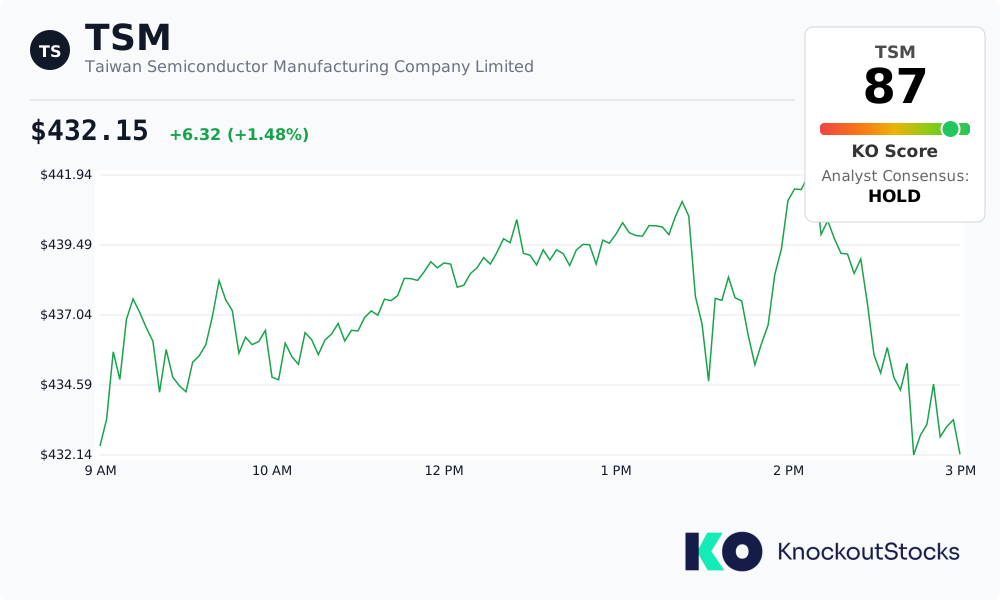 Taiwan Semiconductor Manufacturing Company Limited, TSM
Advanced Vision Semiconductor Manufacturing Corp will serve as the official name for this partnership, with headquarters established in Kumamoto prefecture—the same location where TSMC currently operates its Japan Advanced Semiconductor Manufacturing facility.
Financial contributions will be deployed incrementally, aligned with market dynamics and operational requirements.
Sony Assumes Technology Leadership
According to the partnership terms, Sony will spearhead the development of fundamental image sensor technologies, including strategic product roadmaps and architectural design. TSMC will contribute its semiconductor fabrication expertise and cutting-edge manufacturing processes to enable high-volume production capabilities.
The production facility will specialize in smartphone image sensors. Volume manufacturing is projected to launch in 2029.
Both corporations indicated they’re evaluating supplementary financing options, contingent upon securing Japanese government incentives to achieve maximum planned output.
TSMC’s Strategic Contribution
TSMC’s participation emphasizes manufacturing technology and production expertise rather than product architecture. This framework enables Sony to maintain commercial oversight while utilizing TSMC’s advanced semiconductor fabrication capabilities.
The partnership was initially disclosed in May. Tuesday’s statement provided comprehensive financial terms and official organizational framework.
Sony has been allocating substantial resources toward its imaging sensor division as machine vision applications expand within artificial intelligence ecosystems. This joint operation aims to minimize Sony’s independent capital requirements while simultaneously expanding manufacturing scale.
The Kumamoto site selection leverages TSMC’s current Japanese operations, providing the partnership with immediate infrastructure advantages.
Neither company disclosed specific production volume projections, noting that capital deployment would align with evolving market conditions and operational considerations.
The post TSMC (TSM) and Sony Forge $4.7B Partnership for Advanced Image Sensors in Japan appeared first on Blockonomi.